VTT, Murata
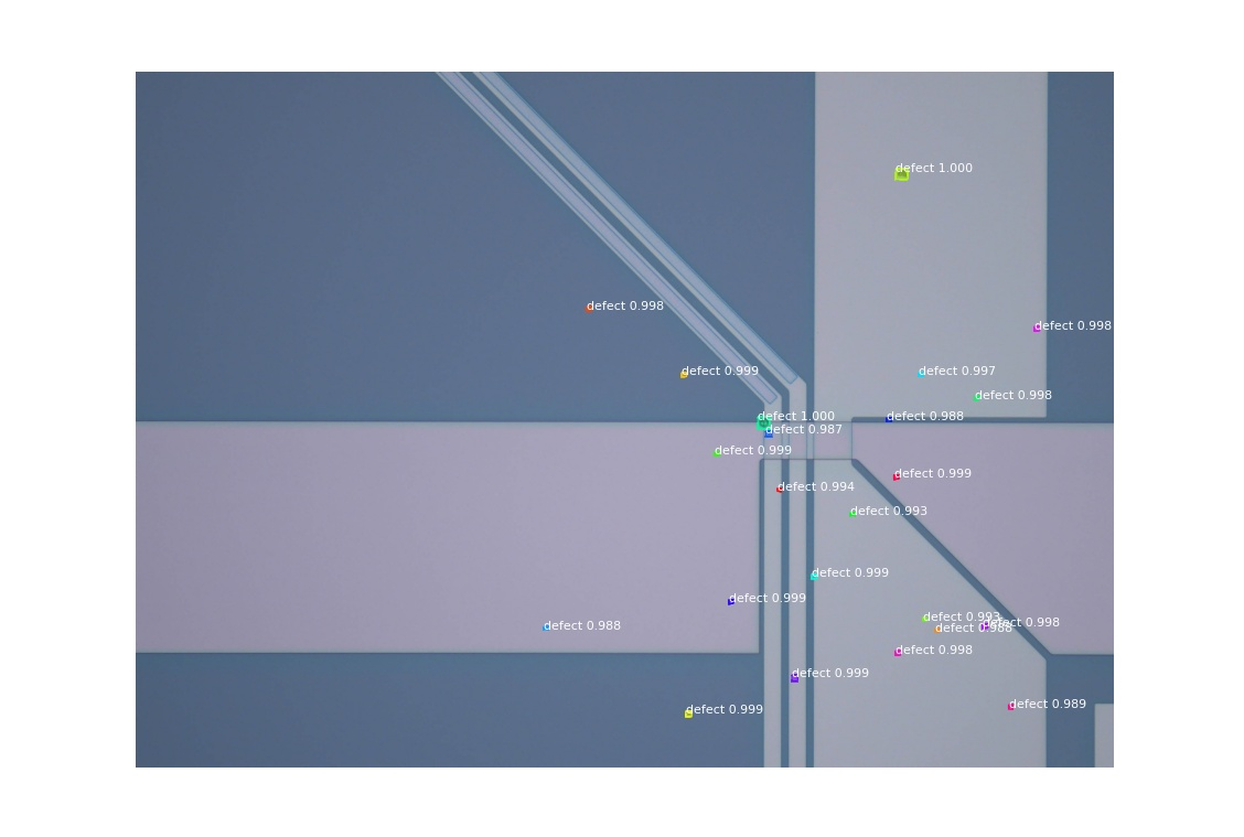
The demonstrator processes the microscopic images of semiconductor wafers and detects surface defects, providing the results in a readable form, either in a table with coordinates and size of each defect or in the form of a heatmap of defect location on a wafer.
Beyond state-of-the-art developments and impacts
New architecture and systems for wafer inspection are developed. Image classification algorithm based on a convolutional neural network (CNN) architecture is trained with images taken by an optical scan of the processed wafers. The type of defect labels images and image coordinates on the wafer are saved, so defects found by the algorithm can be localised, and a map of defects on a wafer can be created. Within the new wafer inspection system, both semantic segmentation and object detection models are applied. Trained models are used to predict defects from data. The algorithm on defect classification will be combined with optical scanning of the wafers to replace manual wafer inspection.

